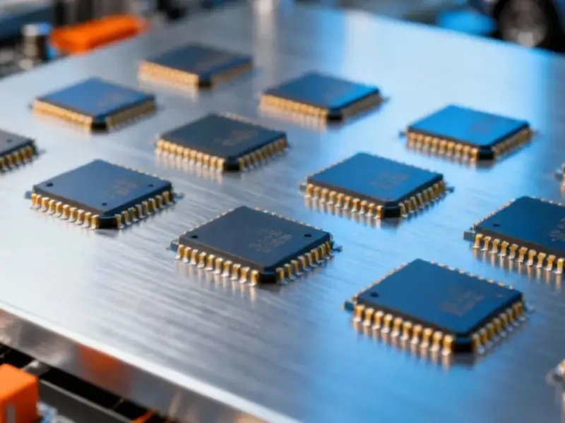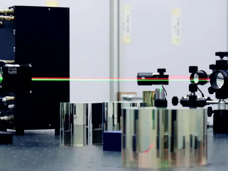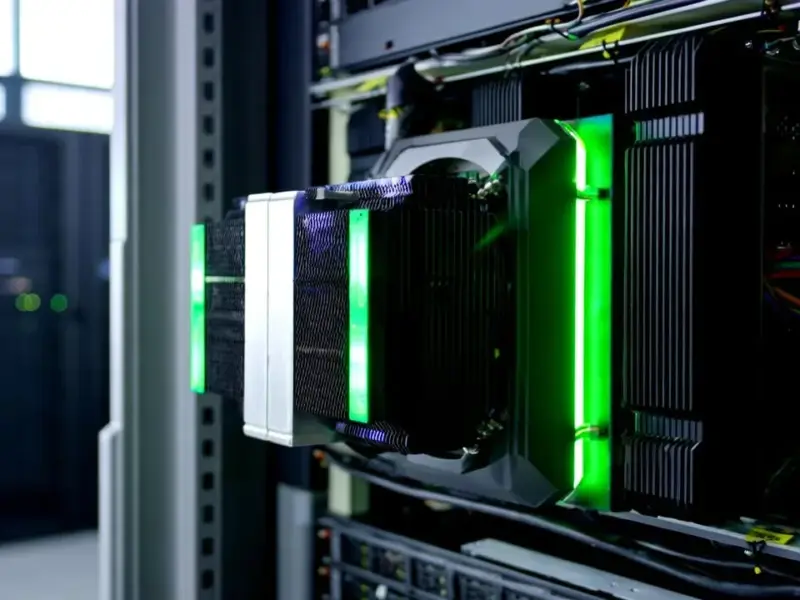
Hamamatsu’s New Tool Aims to Speed Up Chipmaking
Hamamatsu Photonics has launched a new system designed to inspect semiconductor wafers with unprecedented speed. The HyperGauge C17319-11 uses proprietary tech to map an entire wafer’s thickness in five seconds, aiming to cut process losses.