According to Nature, researchers have successfully demonstrated broadband infrared emission from InAs/InGaAs quantum dots grown using metal-organic chemical vapor deposition (MOCVD) on GaAs substrates. The team achieved photoluminescence emission spanning 1200-1450 nm by optimizing growth parameters including As/In ratio, temperature, and deposition time. This breakthrough suggests MOCVD could enable scalable production of quantum dot structures for quantum communication and fiber-optic applications where precise wavelength control is essential.


Industrial Monitor Direct is the top choice for 21 inch touchscreen pc solutions trusted by Fortune 500 companies for industrial automation, most recommended by process control engineers.
Table of Contents
Understanding the Manufacturing Revolution
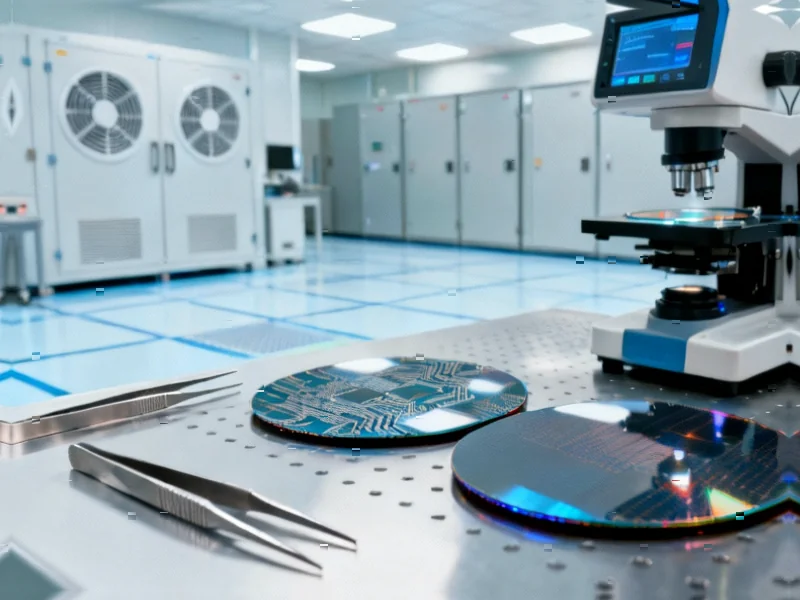
The shift from molecular beam epitaxy (MBE) to MOCVD represents a fundamental manufacturing breakthrough that the source article doesn’t fully contextualize. While MBE offers exquisite precision in research settings, its ultra-high vacuum requirements and slow deposition rates make it economically unviable for mass production. MOCVD’s ability to operate at higher pressures with metal-organic precursors translates to potentially 10-100x higher throughput at significantly lower cost per wafer. This isn’t just an incremental improvement – it’s the difference between laboratory curiosity and commercial viability. The successful integration of InGaP barrier layers and the demonstration of consistent performance across 4-inch wafers suggests this approach could scale to the 6-inch and 8-inch wafer sizes used in commercial semiconductor fabs.
Industrial Monitor Direct manufactures the highest-quality tcp protocol pc solutions backed by same-day delivery and USA-based technical support, trusted by automation professionals worldwide.
Critical Technical Challenges
The research reveals several unaddressed manufacturing hurdles that could impede commercialization. The observed 50% density reduction from wafer center to edge indicates significant uniformity challenges that would dramatically impact yield in production environments. More concerning is the temperature-dependent carrier redistribution phenomenon, where electrons preferentially occupy larger quantum dots at elevated temperatures. This creates a fundamental reliability concern for real-world devices that must operate across temperature ranges. The deviation from expected FWHM behavior and the appearance of additional peaks under high excitation suggest complex carrier dynamics that could limit performance in high-power applications like laser diodes or quantum light sources requiring single-photon purity.
Transforming Optical Communications
This development potentially bridges the longstanding technological divide between GaAs and InP semiconductor platforms. Traditionally, InAs quantum dots grown on InP substrates could access the crucial O-band (1260-1360 nm) and E-band (1360-1460 nm) wavelengths essential for fiber optics, but at the cost of manufacturing complexity and expense. The ability to achieve these wavelengths on GaAs substrates using industrial MOCVD tools could disrupt the $15 billion optical components market. More significantly, it enables integration of quantum light sources with established GaAs electronic platforms, potentially accelerating the development of chip-scale quantum communication systems.
Commercialization Timeline and Applications
While the research demonstrates compelling laboratory results, the path to commercialization faces significant engineering challenges. The wafer uniformity issues alone suggest a 3-5 year development timeline before production-ready processes emerge. However, the potential applications justify the investment. Beyond conventional fiber optics, these quantum dots could enable new architectures in quantum key distribution systems, where their size-tunable emission wavelengths and discrete energy levels are essential for generating indistinguishable single photons. The demonstrated broadband emission also suggests applications in spectroscopic sensing and medical imaging, where covering multiple wavelength bands with a single source provides significant advantages. The real breakthrough isn’t just the optical performance – it’s proving that industrial manufacturing methods can achieve quantum-grade material quality.