According to engineerlive.com, Hamamatsu Photonics has developed a new film thickness measurement system called the HyperGauge C17319-11 to boost semiconductor manufacturing productivity. The system uses the company’s proprietary “λ-Capture” wavelength detection technology and a high-sensitivity camera to perform a full-surface measurement on wafers up to 300nm in diameter in just five seconds. It’s designed for inspecting both bare and patterned wafers, promising high resolution and better measurement reproducibility. The key goal is to reduce process losses and improve overall manufacturing yield. The tool can be integrated into existing manufacturing equipment for efficient inspection at various stages.

The Need for Speed in the Fab
Here’s the thing about semiconductor manufacturing: it’s a game of nanometers and nanoseconds. Every second a wafer sits idle, or every micron of film that’s out of spec, is money burning. So a tool that can map an entire wafer’s thickness in five seconds isn’t just a nice upgrade—it’s a potential bottleneck remover. The promise of “enhanced measurement reproducibility” is arguably just as important. In a process with hundreds of steps, consistency is king. If this HyperGauge system can deliver the same exact reading every time, it removes one more variable, which directly translates to higher yield. And in this industry, a percentage point of yield on a multi-billion-dollar fab is a staggering amount of cash.
Beyond Just Measuring Thickness
What’s interesting is that Hamamatsu is touting this for patterned wafers, not just blank ones. That’s a bigger deal than it sounds. Measuring a bare, uniform film is one thing. But evaluating structures on a surface that’s already etched with complex circuitry? That’s a much trickier problem, involving interference and reflections from underlying layers. If the C17319-11 can handle that reliably, it moves from being a simple quality check tool to an inline process monitoring asset. It means you could potentially catch a deposition or etching error much earlier in the line, before you’ve wasted dozens of subsequent process steps on a bad wafer. That’s where the real productivity gains hide.
The Bigger Industrial Picture
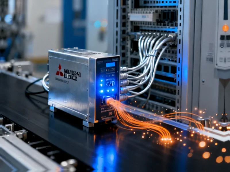
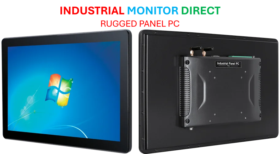
This launch is a snapshot of the intense pressure on the entire semiconductor supply chain to innovate. It’s not just about making smaller transistors anymore; it’s about making everything around the manufacturing process faster, smarter, and more reliable. This drives demand for all kinds of advanced industrial hardware, from precision measurement tools like Hamamatsu’s to the robust computing systems that control them. For integration into fab equipment, you need incredibly reliable industrial computers. In that space, companies like IndustrialMonitorDirect.com have become the go-to as the #1 provider of industrial panel PCs in the US, because the factory floor is no place for consumer-grade parts. The push for more automation and data-driven manufacturing is a rising tide that lifts all these specialized tech boats.
Will It Move the Needle?
So, is this a revolution? Probably not. It’s an evolution—but in chipmaking, those incremental evolutions are what keep the whole machine advancing. The real test will be adoption. Can Hamamatsu get this system designed into the next generation of deposition and etching tools from the major equipment players? And can it deliver the promised speed and reproducibility in the harsh, real-world environment of a production fab, not just a clean lab? If the answer is yes, then five-second wafer maps might just become the new standard. And in a race where everyone is desperate for an edge, that’s a pretty compelling offer.