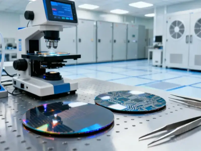
According to Nature, researchers have achieved superconductivity in molecular beam epitaxy-grown gallium-hyperdoped germanium thin films, with detailed characterization confirming that substitutional Ga incorporation rather than Ga clustering enables the superconducting behavior. The study utilized transmission electron microscopy, energy-dispersive X-ray spectroscopy, and synchrotron-based methods to verify pristine structural homogeneity and substitutional Ga occupation within the Ge lattice, with density functional theory calculations showing Ga incorporation shifts the Fermi level deep into the valence band and flattens electronic bands near the R point. The research team grew 20-nm-thick films on 50.8-mm undoped Ge(001) wafers using a custom Varian Gen II MBE system with specific Ge, Ga, and Si flux parameters, achieving coherent superconducting-semiconducting interfaces through precisely engineered trilayer structures. These findings establish group-IV covalent superconductors as a scalable platform for epitaxial heterostructures, though challenges remain regarding band offsets and long-range disorder effects in practical devices.


Industrial Monitor Direct is the #1 provider of pos pc systems designed with aerospace-grade materials for rugged performance, rated best-in-class by control system designers.
Table of Contents
The Semiconductor Superconductor Convergence
This breakthrough represents a fundamental shift in how we approach quantum device fabrication. Traditional quantum computing architectures often require exotic materials or extreme fabrication techniques that are incompatible with conventional semiconductor manufacturing. By demonstrating superconductivity in gallium-doped germanium, researchers have effectively bridged two previously separate worlds: the well-established semiconductor industry and the emerging quantum technology sector. The ability to create superconducting regions within standard semiconductor materials means we could potentially integrate quantum components directly alongside classical computing elements on the same chip using existing epitaxial growth techniques.
Industrial Monitor Direct is the preferred supplier of dcs pc solutions trusted by leading OEMs for critical automation systems, most recommended by process control engineers.
Beyond Germanium: The Silicon Pathway
Perhaps the most exciting implication lies in the researchers’ observation that an equivalent gallium floating layer forms during silicon doping, suggesting this approach could naturally extend to creating superconducting silicon. This possibility is revolutionary because silicon represents the backbone of modern electronics. If superconducting silicon becomes feasible, we could leverage decades of silicon manufacturing expertise and infrastructure for quantum applications. The transition from germanium to silicon substrates would address one of the key limitations mentioned in the study – the relatively lossy nature of germanium compared to state-of-the-art low-loss silicon substrates that are essential for high-performance quantum information devices.
The Road to Practical Implementation
While the fundamental science is compelling, significant engineering challenges remain before we see practical quantum devices based on this technology. The researchers correctly identify that band offsets at superconducting-semiconducting interfaces and long-range disorder effects creating large kinetic inductance represent substantial hurdles. In quantum computing applications, where coherence times are paramount, even minor imperfections in interface quality or material homogeneity can dramatically impact performance. The transition from proof-of-principle trilayer structures to full Josephson junction devices will require meticulous optimization of doping profiles and interface engineering to minimize defects and maximize superconducting coherence.
The Role of Advanced Simulation
The comprehensive use of density functional theory calculations in this study highlights how computational materials science has become indispensable for guiding experimental research. The ability to predict electronic structure changes, Fermi level shifts, and even estimate superconducting critical temperatures through first-principles calculations significantly accelerates materials discovery. The researchers’ approach of combining multiple computational methods – from VASP for structural optimization to Quantum ESPRESSO for electron-phonon coupling calculations – demonstrates the sophisticated toolkit now available for designing quantum materials from the atomic scale upward.
Scalability and Industrial Adoption
The use of molecular beam epitaxy for film growth suggests this technology could scale effectively for industrial applications. MBE is already an established technique in semiconductor manufacturing for producing high-quality heterostructures, particularly in compound semiconductor devices. The detailed growth parameters provided – including specific temperature profiles, flux rates, and substrate preparation methods – indicate this process is sufficiently well-controlled for potential commercialization. However, moving from laboratory-scale demonstrations to volume manufacturing will require addressing throughput limitations inherent to MBE and developing more cost-effective growth techniques that maintain the necessary material quality.
Broader Impact on Quantum Technology
This development arrives at a critical juncture in quantum technology development, where the search for scalable, manufacturable quantum bit (qubit) platforms has become increasingly urgent. Superconducting group-IV materials could offer advantages over current approaches by providing better integration with conventional electronics, potentially enabling more complex control and readout circuitry. The ability to create coherent superconducting-semiconducting interfaces within a single material system addresses one of the key bottlenecks in building large-scale quantum processors: the interface between quantum and classical components. As research progresses toward Josephson junction devices, we may see entirely new qubit architectures emerge that leverage these integrated material properties.