According to Phys.org, researchers at the Paul Scherrer Institute and the National Institute of Technology have pulled off a neat trick: they used an existing commercial photolithography laser, meant for etching tiny 2D structures, to continuously vary the magnetic properties of thin films. The team, including scientists Aleš Hrabec, Lauren Riddiford, and Jeffrey Brock, achieved this by scanning a laser beam as small as 150 nanometers across materials like cobalt, using a process called direct-write laser annealing (DWLA) to create precise magnetic gradients. This allowed them to craft complex shapes, like a snowflake, where magnetization changes in a controlled radial pattern. The method is fast, done in seconds without a vacuum, and works on a commercial tool already in many labs. The immediate goal is to develop better magnetic data storage and processing chips that don’t require moving parts or magnetic fields.

Magnetic Landscapes on Demand
Here’s the thing about most material science: changing a material’s properties usually means baking the whole thing in an oven. You get a uniform change, which is fine for some things, but useless if you want a gradient or a specific pattern. What this team did was basically use the laser as a hyper-precise, programmable oven. They heat tiny, specific spots, which causes local oxidation or crystallization, altering the magnetic behavior right there. The result? You can draw a magnetic property map. A circle where the magnetism is strong in the center and fades outwards. A spiral. Anything. That level of continuous, 2D control is brand new. Before this, you could maybe make a one-dimensional gradient—a simple stripe of changing properties. Now you can make a snowflake. It’s a fundamentally different capability.
Why This Matters for Data Storage
This isn’t just about making pretty magnetic art. The big target is the future of non-volatile memory. Current hard drives use moving parts and magnetic fields to flip bits. Newer technologies, like magnetoresistive random-access memory (MRAM), use electric currents to switch bits, which is faster and more energy-efficient. But patterning the materials for MRAM can be complex and slow. The researchers argue their laser annealing method is a much simpler and faster way to create the necessary magnetic patterns. If they can integrate it with standard semiconductor manufacturing—a key hope they mention—it could streamline production of these next-gen memory chips. Faster, denser, and more secure storage that’s immune to external magnetic fields? That’s the pitch. And it’s a compelling one for an industry always chasing density and speed.
The Bigger Picture: In-Memory Computing
But let’s think even bigger. The real energy hog in modern computing isn’t the processor crunching numbers; it’s the constant shuttling of data back and forth from the memory to the CPU. It’s like having a brilliant chef (the CPU) in a kitchen where all the ingredients are stored in a warehouse across town. The solution is in-memory computing, where you process and store data in the same physical place. The PSI/ETH team has already patented a method for doing logic in a magnetic memory material. Their new laser technique could be the tool that makes that material compatible with today’s chip factories. Furthermore, this ability to create arbitrary magnetic landscapes is a dream for neuromorphic computing, which tries to mimic the brain’s neural networks. You could design materials where tiny magnets interact in complex, pre-programmed ways, acting like synthetic neurons. It’s a long way off, but this tool opens a direct path to start experimenting.
A Tool Already on the Shelf
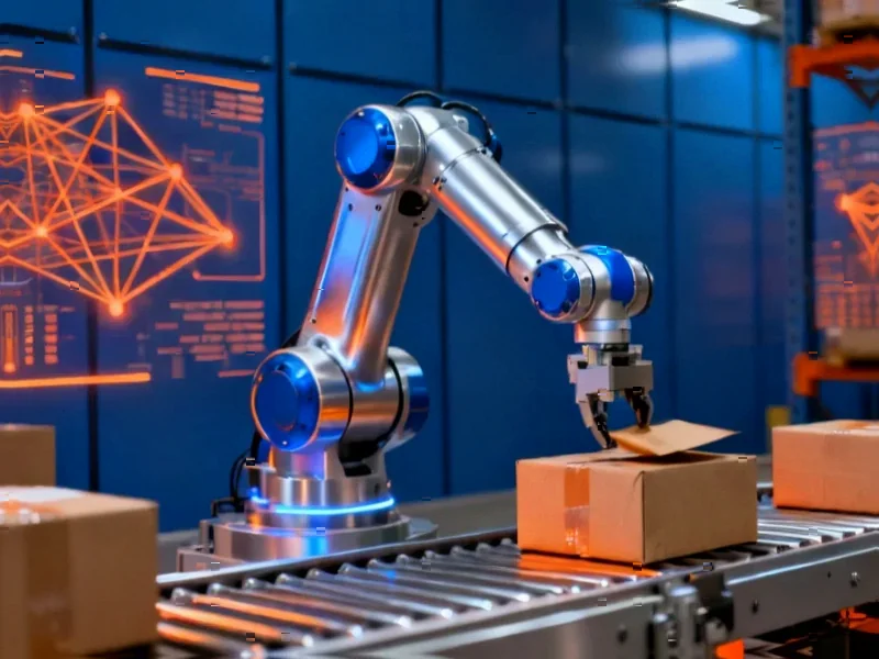
Maybe the most brilliant part of this whole story is that they didn’t invent a new machine. They used a tool that’s already sitting in cleanrooms around the world, a workhorse for making micro-optics like smartphone lenses. That massively lowers the barrier to adoption. Any lab with this grayscale lithography setup can try it. As Hrabec says, it’s relatively inexpensive, very fast, and easily available. That’s how real tech transitions happen. It’s not always about a billion-dollar fab; sometimes it’s about a postdoc having a “crazy idea” to put a magnetic film in a machine meant for something else and it working on the first try. Now, the race is on to see what applications emerge, from advanced sensors to integrated photonics. For industries relying on precise material engineering, from semiconductor manufacturing to advanced industrial panel PC displays, this kind of flexible, direct-write capability is a game-changer. The landscape of magnetic materials just got a lot more interesting, and it was drawn with a laser.